1. Introduction
Semiconductor crystals of indium selenides (In4Se3, InSe) and their surfaces continue to attract the attention of researchers due to their non-trivial anisotropic properties [1-3]. These compounds crystallize into layered structures with individual layers that possess a high degree of individuality. This causes not only the anisotropy of the electronic spectra of their surfaces and many physical properties, but also gives rise to certain peculiarities in the surface structure – grooves with chain-like structures for the (100) In4Se3 surface. The intercalation of crystals makes it possible to systematically control the electronic properties of their surfaces, through surface heterization and the formation of periodically doped structures on the surfaces [4, 5], formation of surface nanowires and quantum dots. Crystalline In4Se3 is a complex semiconductor system in which, in addition to the 3D system, the properties of low-dimensional 2D and even 1D [1-3] nanosystems are combined (Fig. 1).
In4Se3 are of interest and possess the properties suitable for devices at transistor widths in the region of 10 nm depends on the facility with which such materials can be manipulated as a 2D material, and adapted to large scale manufacturing [1-5]. In4Se3 is a semiconducting crystal with a layered structure [5–7]. The intralayer interactions in this system are of the strong ionic-covalent kind, whereas the interlayer interactions are of the weaker kind. This system’s (100) surface is found to be corrugated (and not smooth) [5-9], which results in structures having quasi-1D chains at the semiconducting surface of In4Se3 (100) system (see Fig. 1)
Additionally, this system is proven to have a band structure that is extremely anisotropic in nature [10–13]; and is found to be dominated by multivalent indium [(In3)5+] bonded with selenium through covalent-ionic bonds. Furthermore, its band gap (0,68 eV) – which is of the direct kind – is comparable to that of silicon’s (1.1 eV) as it dependend from concentration impyrites [10,11]. However, the transport measurements dictate that the band gap is about 0.6 eV [13]. Valence band is discovered to be placed well below the Fermi level, as is evident from the angle resolved valence band UPS spectroscopy data [19]. Thus, it is suggested that In4Se3(100) is an n-type semiconductor, making it consistent with the transistor measurements [3].
2. Experimental methods
The In4Se3 single crystals were grown by Czochralski method in a restored hydrogen atmosphere from the melt-solution of synthesized alloy In4Se3+10 at.% In with an over-stoichiometric In (£10 at.%) as a solvent. Synthesis alloy In4Se3+10 at.% In for the growing crystals In4Se3 were made by the melting of the components in evacuated quartz ampoules. In4Se3 crystals grown by Czochralski method from In4Se3 with up to 10 atomic percent In alloy were always self n-doped by In (n-type conductivity) with a carrier concentration of 1015/1018 cm-3 (0.01/0.11 (Ohm·cm)-1 the low/high conductivity).
In4Se3 semiconductor crystals crystallized in the orthorhombic system and had a pronounced layered structure, whereas the layers had a complicated structure (Fig. 1 (left)). In4Se3 semiconductor layered crystals were characterized by rather a strong anisotropy of their physical properties, which should be directly reflected in the anisotropy and the features of properties for the cleaved surfaces (100) [4-6].
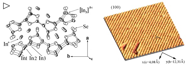

Fig.1. (for the left) Fragments of the In4Se3 layered crystal structure (projection onto the (001) plane) and its interlayer cleavage surface (100). The triangle in the upper left part indicates the direction of cleavage. [In3]5+– indium polycation (In1, In2, In3) in the layer; In+– is an indium cation between the layers [9]. (for the right) Fragments of the STM image of UHV cleavage surface (36´36 nm2) with chains and furrows along х(с) direction (acquired at constant current Іt=150 pA with Vb=2 V bias and T=80 K). Lattice constants: a=15,297(1)Å; b=12,308(1) Å; c=4,0810(5) Å due to ХRD data.
The peculiarities of In4Se3 crystal bulk 3D system electron-energetic structure that appear as a result of its layered structure were discussed by Bercha et al [13, 15, 16]. In addition of localized states (LS) of the impurity nature, as a result by self-doped and self-intercalated by In, the quasi-localized states (QLS) of the Mott type near the Fermi level exist. These QLS appear as a result of the influence of the oscillation of the layers on the electronic subsystem of crystal. The bulk Mott QLS concentration is Nt »NF×DE (Nt»(4-8)×1017 cm-3), where DE»0.15-0.20 eV is the width of QLS band near the Fermi level and NF »(3¸5)×1018 eV-1×cm-3 is the density of states [16, 17].
In4Se3 crystal bulk optical width of energy gap Eg»0.65¸0.67 eV [13] and Fermi level EF is 0.17-0.22 eV below the bottom of conduction band and electron affinity c is equal to 3.2-3.5 eV. The existence of Mott type QLS, in the result of dynamic disordered state of the layered crystals, and LS of impurity nature, leads to peculiarities in their occupancy, i.e. the possibility of electron jumps on states that are close to EF. Therefore, as occupied as free energetic states exist near Fermi level in In4Se3 crystal at 293 K and determine the peculiarities of its cleavage surface's adsorption activity [17] and another’s electronic properties of cleavage surfaces.
It is well known that, due to the relatively weak interlayer bonding, In4Se3 layered semiconductor crystal samples cleave along the interlayer spaces (see Fig. 1 (left) and triangle in upper). The striking feature of the In4Se3 (100) surface is the furrowed and chainlike anisotropic relief, as could be seen after inspection of bulk crystal and energetic structure [11, 18]. The approximately two-dimensional (2D) cleavage surface of layered (100)-oriented In4Se3 crystals arouses great interest for its potential utilization as template in nanodevice fabrication on nanometre scale, e.g. of nanowires [4-8]. Besides, layered In4Se3 crystals have become an attractive subject for practical applications as thermoelectric materials, which exploit intrinsic nanostructure bulk properties induced by charge density waves [19]. The “large” cleavage areas of In4Se3 usually show a small number of topographic steps with a height corresponding to the thickness of one or a few layers in scanning tunnelling microscopy (STM) images. STM has the unique ability to reveal structural and electronic information of the surface on the atomic scale. STM images display the geometric structure of the surface, but also depend on the electronic density of states of the sample, as well as on the complex tip sample interaction mechanisms. In the present work, we employed STM and scanning tunnelling spectroscopy (STS) to study the In4Se3 (100) cleavage.
Layered crystals of In4Se3 (samples 3´6´4 mm3, with a special shape for in situ cleavage) were grown by the Czochralski method. In4Se3 samples were naturally (through the phenomena of indium self-intercalation) n-doped with a carrier concentration more than 1016 cm-3. The samples were cleaved in situ at room temperature in an ultra high vacuum (UHV) chamber and in air ex situ, using a stainless steel tip. An Omicron NanoTechnology STM/AFM System under UHV (3 10-11 Torr) was used. An STM/STS investigation of the In4Se3 (100) crystal was carried out to yield the topography, I–V characteristics, and dI/dV and normalized dI/dV versus V. The STM images were collected in the constant tunneling current mode. To visualize the measured STM and STS data we applied the computer program WSxM v.4.0 designed by Nanotec Electronica [20]. The cleaved crystals were examined in over paper [2], using X-ray photoemission spectroscopy (XPS). The core level XPS measurements were carried out using a SPECS X-ray Al anode (hv=1486.6 eV) source and a hemispherical electron energy analyzer. Samples were cooled between 240 and 300 K.
3. Results and discussion
Since the tip probe is sensitive to locations into (or out of) which electrons can tunnel, STM images are pictures of the local density of states (LDOS) at the surface. These states may, or may not correspond to actual atomic positions. Special care must be taken to isolate the STM from environmental influences such as floor vibrations. Operation under UHV eliminates surface contaminates that interfere with the stability of the tunneling process.
We now turn to some remarkable features appearing in In4Se3 (100) surface STM images. Figs. 2 show typical constant current STM images of an In4Se3 (100) UHV cleavage surface 50´50 nm2, obtained with a bias voltage +1.5 V (0.031 nA) (thus corresponding to electrons tunneling from the probe-tip into normally empty states of the sample) and –1.5 V (0.114 nA) (vice versa tunneling). The STM images were filtered applying a 2D Fast Fourier Transform (FFT) to reveal the periodical structure of the surface, and subsequent profiling gave periodicity distances of about 1.3-1.4 nm and 0.4 nm. These values are in good agreement with the lattice parameters normal and parallel, respectively, to the furrows or chains on the cleavage surface, derived by “bulk” (X-ray diffraction) [1] or “surface” (low-energy electron diffraction (LEED), atomic force microscopy (AFM)) studies [3,6].
It was relatively difficult to obtain sufficient lattice resolution when acquiring the STS spectra. This may be due to the presence of intercalated indium, which is not connected with specific lattice sites, on the cleavage plane. The latter can be clearly seen when considering local STS spectra of the UHV cleavages.
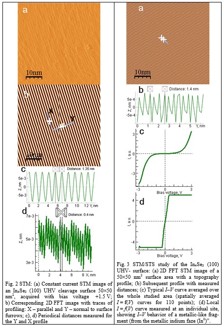

We mapped the local differential conductance of the surface simultaneously with topographic measurements. Fig. 3a shows a 2D FFT image of the UHV cleavage that reveals a periodic lattice structure corresponding to the In4Se3 (100) surface (Fig. 3b) shows the subsequent profile with measured surface distances). Current-imaging-tunneling spectroscopy (CITS) is an STS technique where an I–V curve is recorded at each pixel in the STM topography. Measuring local CITS curves allows characterizing the variation of the local electronic structure. The dI/dV versus voltage bias V(dI(V)/dV = f(V)) curve is proportional to LDOS. Since the tunneling current in a scanning tunneling microscope only flows in a region with a diameter of ~5 A, STS is unusual in comparison with other surface spectroscopy techniques, such as ultraviolet photoelectron spectroscopy, which average over a larger surface region. STS measurements, averaged over the whole studied sample surface, revealed mainly semiconductor-like behavior (I = f(V)) (see Fig. 3c). But, as shown in Fig. 3d, in local spectra we were able to distinguish regions of slightly different electronic properties, towards metallic-like behavior.
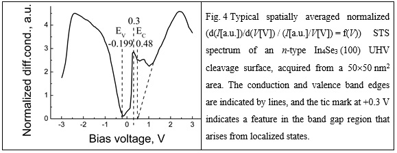
Fig. 4 shows a typical averaged normalized d(I[a.u.])/d(V[V]) / (I[a.u.]/V[V]) = f(V) STS spectrum of an n-type In4Se3 (100) surface, obtained from a 50´50 nm2 area of a In4Se3 cleavage in UHV. This spectrum was acquired as CITS data and normalized by WSxM software. The conduction band and valence band components in the conductance are clearly seen, and the band edges are marked in the spectrum.

We define the band gap as the separation between these band edges, yielding an observed value of 0.68 eV for this spectrum. The value Еg=0.68 eV, obtained for In4Se3 (n-type conductivity, n»5´1015-1017 cm-3 at 300 K) by STS, satisfactorily agrees with the values Eg»0.62-0.67 eV obtained for bulk In4Se3 layered semiconductor crystals by other experimental and theoretical methods [7,8]. In particular, this similarity correlates with the stability and the lack of reconstruction of the In4Se3 (100) surface structure.
Besides, conduction and optical absorption experiments [9] have shown that for In4Se3 n-type layered crystals, so-called low compensated samples, the donor levels lie 0.17-0.18 eV below the conduction band. But in all cases, an energy gap cleavage surface In4Se3 (100) clearly observed and corresponding the gap bulk crystalline In4Se3.
4. Conclusion
The appearance of new energy states and bands in the electronic energy structure of (100) In4Se3 surfaces is due to the presence of segregated indium atoms on the surface, which appear as localized states of high density, similar to the case in the bulk. The main confirmation of this is the applied STS method, which is a method of spectroscopy of the electronic energy structure of the surface. In addition, the presence of segregated metallic In atoms on the (100) surface of In4Se3 was also proven in our work [2] by the XPS method during the heat treatment of surfaces. Surface segregation of excess indium on the (100) In4Se3 surface, which is caused by self-intercalation of the crystal bulk during growth and heat treatment, was detected in the STS and XPS spectra.
References
1. Vorobeva N.S., Lipatov A., Torres A., Angel Torres, Jun Dai, Jehad Abourahma, Duy Le, Archit Dhingra, Simeon J. Gilbert, Galiy Pavlo V., Nenchuk Taras M. et al. // Advanced Functional Materials. – 2021. – Vol. 31, Is. 52, P. 2106459 (11pp)
2. Dhingra A., Marzouk Z.G., Mishra E. Galiy P.V., Nenchuk T M., Dowben Peter A. // Physica B: Condensed Matter. – 2020. -Vol. 593, - P. 412280-412282.
3. Dhingra A., Galiy P.V., Wang Lu, Vorobeva N.S., Lipatov A., Torres Angel, Nenchuk T M. et al. // Semicond. Sci. Technol. . – 2020.-Vol. 35, P. 065009, (9pp)
4. Galiy P.V., Mazur P., Ciszewski A., Nenchuk T.M., Yarovets' I.R. // The European Physical Journal Plus. – 2019. -Vol. 134, Is. 2. - P. 70-75.
5. Galiy P.V., Nenchuk T.M., Mazur P. et al. // Applied Nanoscience. - 2020. - Vol. 10, Is. 12. - P. 4629-4635.
6 Galiy P.V., Musyanovych A.V., Buzhuk Ya.M. // Physica E: Low-dimensional Systems and Nanostructures. – 2006. -Vol. 135, Is. 1. - P. 88-92.
7. Galiy P.V., Nenchuk T.M., Stakhira J.M., Fiyala Ya.M. // Journal of electron spectroscopy and related phenomena. - 1999. - Vol. 105, No 1. - P. 91-97.
8. Galiy P.V., Nenchuk T.M., Dveriy O.R., Ciszewski A., Mazur P., Zuber S. // Physica E: Low-dimensional Systems and Nanostructures Vol. 41/ No 3, P. 91-97, 465-469
9. Schwarz U., Hillebrecht H., Deiseroth H.J., et al.., Z. Kristallog. 210 (1995) 342-347
10. Losovyj Y.B., Klinke M., Cai E., Rodriguez I., Zhang J., Makinistian L., Petukhov A. G., Albanesi E.A., Galiy P.V., Fiyala Ya, Liu J., et al.., Appl. Phys. Lett. 92 (2008),
11. Losovyj Y.B., Makinistian L.,. Albanesi E.A, Petukhov A.G., Liu J., Galiy P.V., Dveriy O. R., Dowben P.A., J. Appl. Phys. 104 (2008),.
12. Fukutani K. Miyata Y., Matsuzaki I., Galiy P.V., Dowben P.A., Sato T, Takahashi T., // J. Phys, Soc. Jpn 84 (2015) 1–6..
13. Bercha D.M., Mitin O.B., Kharkhalis L. Yu, et al.. // Phys. Solid State 37 (1995) 1778–1781.
14. Fukutani K., Sato T., Galiy P.V., Sugawara K., Takahashi T. // Phys. Rev.B – 2016 Vol. 93, Is 20, P.205156
15. Sznajder M.,. Rushchanskii K.Z, Kharkhalis L.Yu., Bercha D.M., Phys. Status Solidi B 243 (3) (2006) 592-609.
16. Demkiv L.S., Demkiv T.M., Savchyn V.P., Stakhira J.M., Journal of Physical Studies 2(4) (1998) 536-540.
17. Galiy P.V., Nenchuk T.M., Stakhira J.M. // Journal of Physics D: Applied Physics. 2001, Vol.34, Is.1, P.18-24.
18. Galiy P., Nenchuk T., Losovyj Ya.B., Fiyala Ya.M., Funct. Mater. 15 (2008) 68-73.
19. Rhyee J.-S., Lee K.H., Lee S.M., Cho E., Kim S.I., Lee E., Kwon Y.S.,. Shim J.H, Kotliar G., Nature 459 (2009) 965-968.
20. Horcas I., Fernandez R., Gomez-Rodriguez J.M., Colchero J., Gomez-Herrero J. et al.., Rev. Sci. Instrum. 78 (2007) 013705-013708 (WSxM©; http://www.nanotec.es).
|